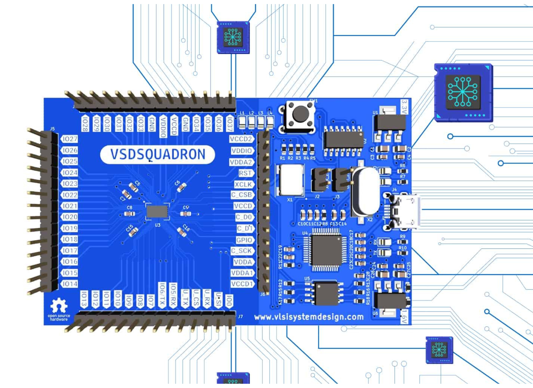
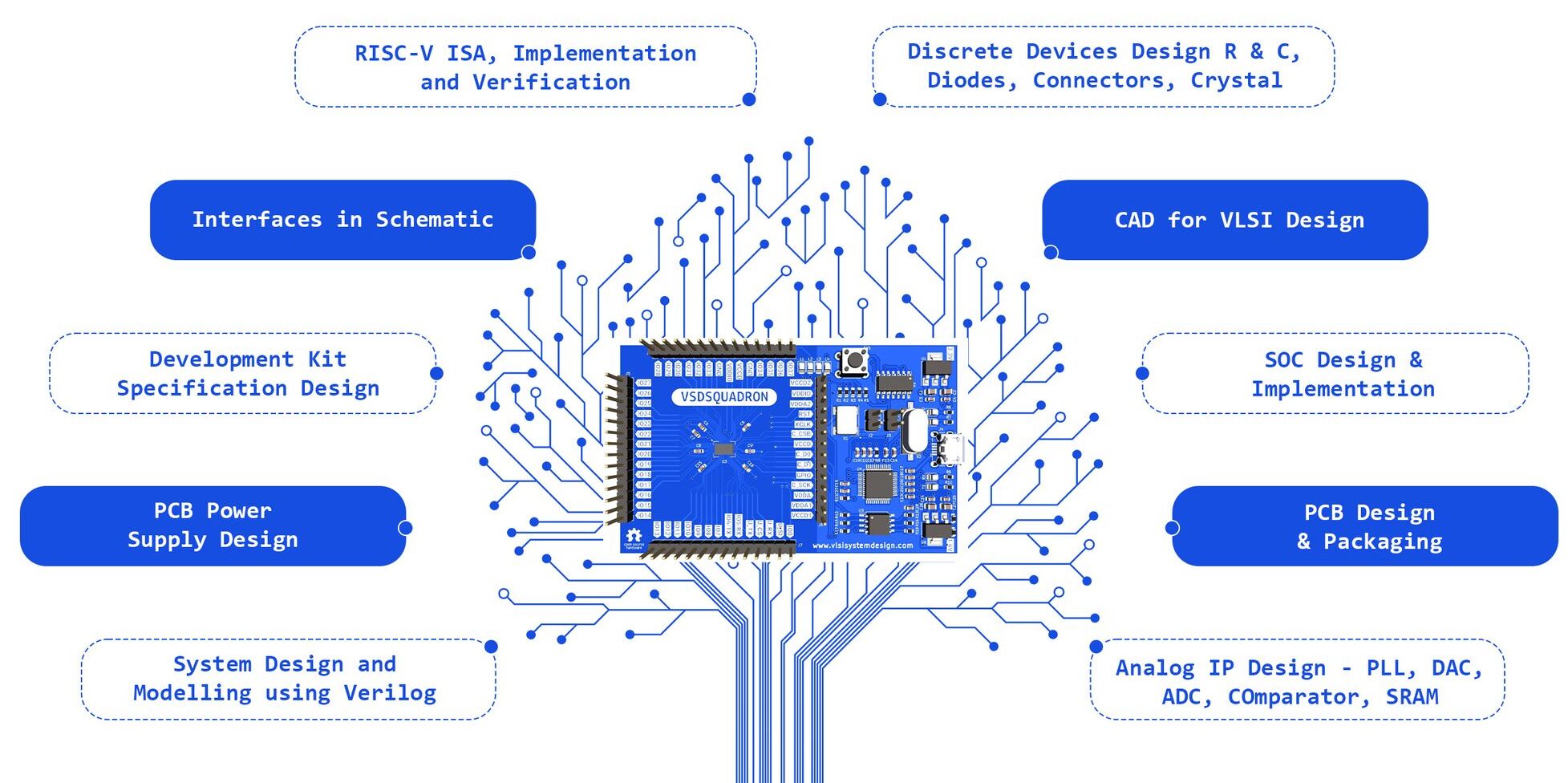


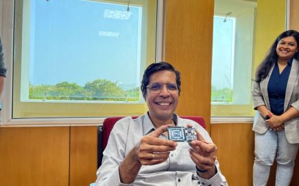
“VSDSquadron”: Empowering Learners with Open-Source Technology and VLSI/RISC-V Skills
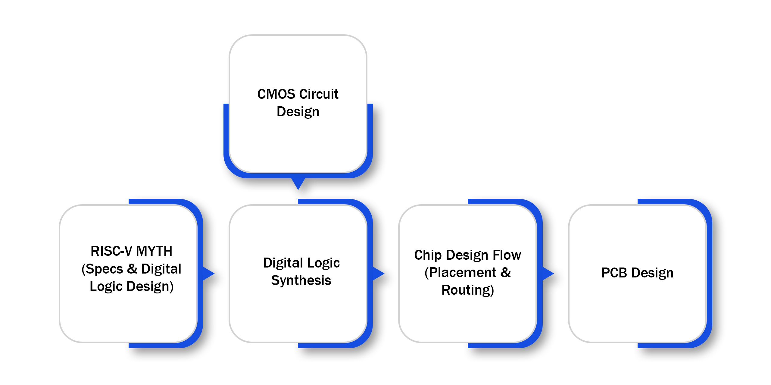
Embedded and Chip design Education curriculum – All in one via VSDSquadron
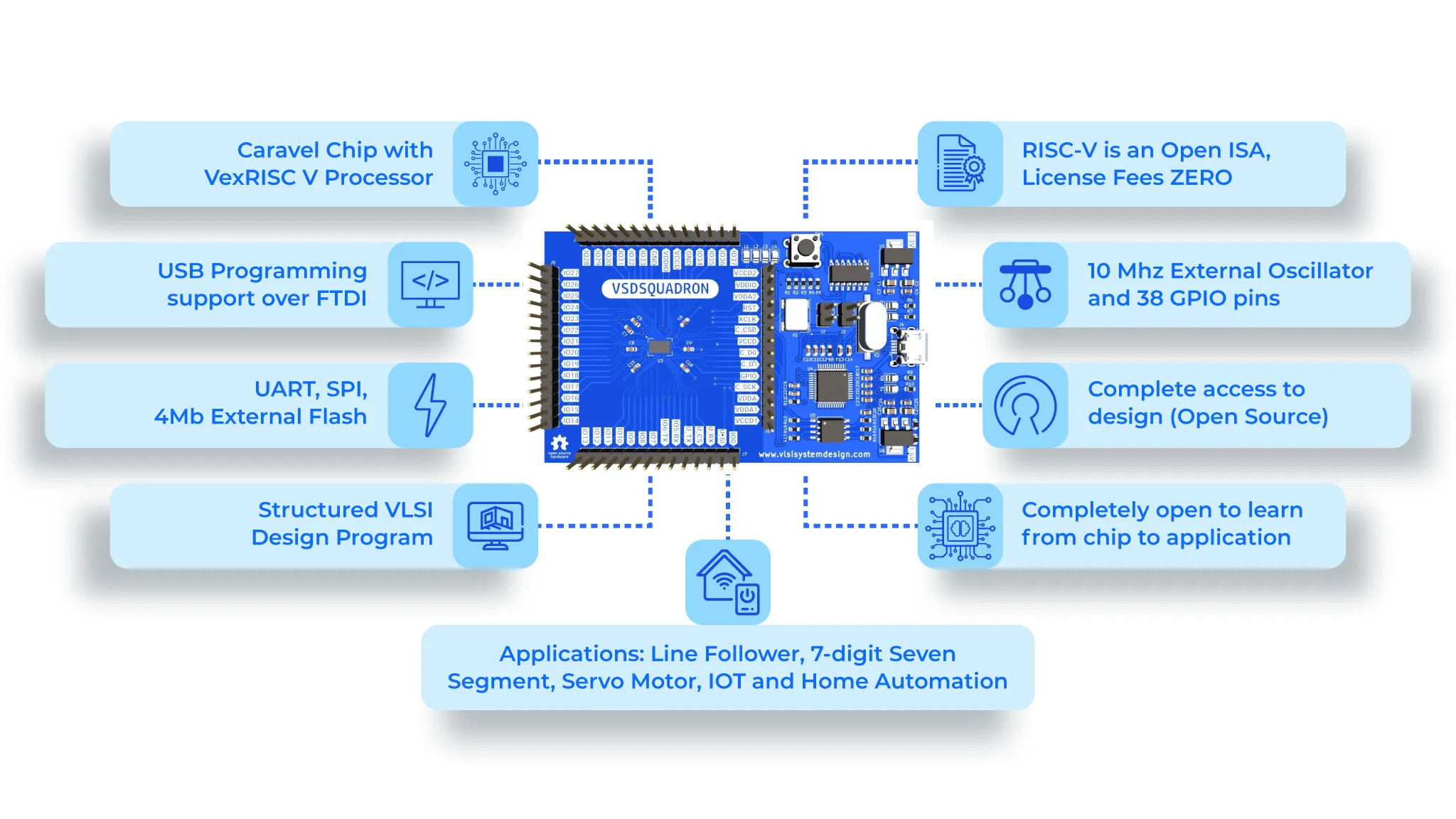
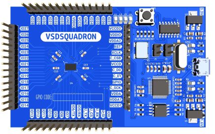
Five reasons why you need VLSI and RISC-V education board ‘VSDSquadron’
Innovation & Education Unite
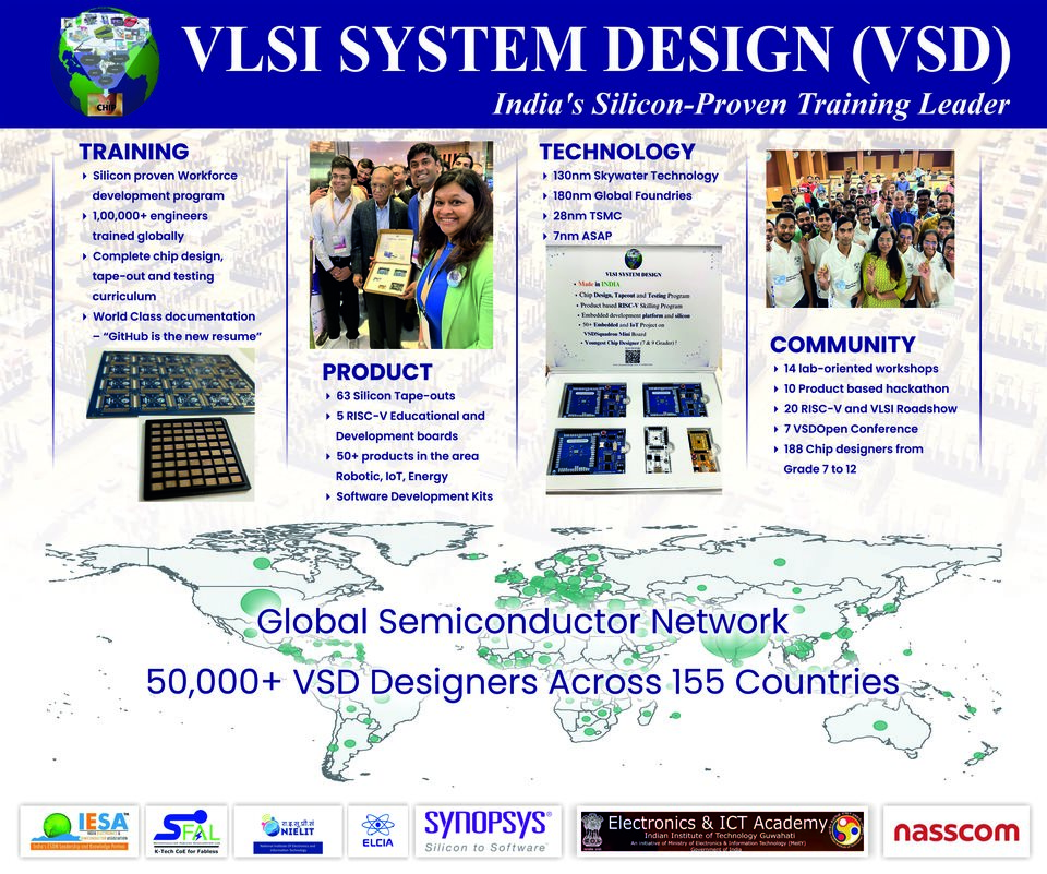
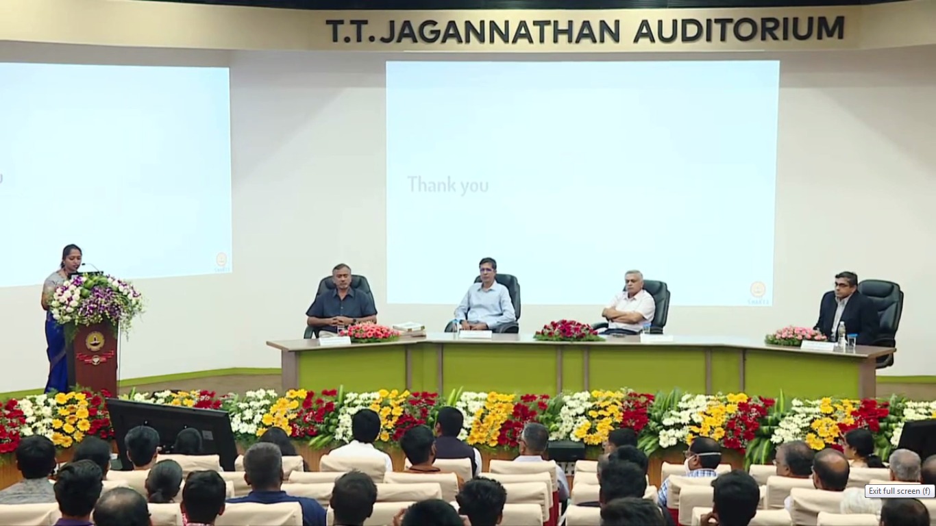
VSD Launches VSDSquadron In Collaboration With IIT Madras & DIR-V

Unleashing VLSI
Job Roles, Convergence With Embedded Systems, and Startups
Semicon India Future Skills by IESA
VSD showcased at Semicon India 2023

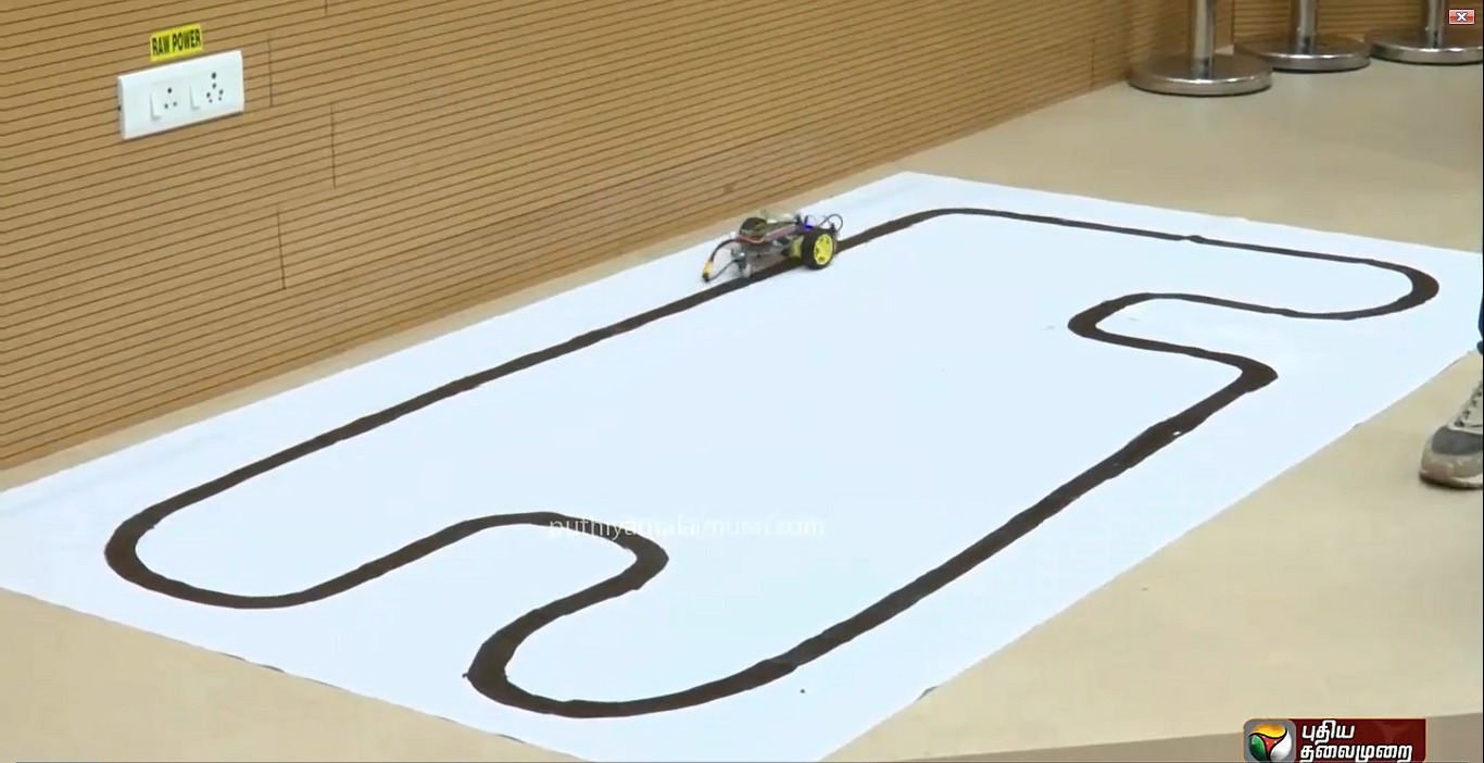
Puthiya Thalaimurai
VSDSquadron Educational board on Tamil News channel
NIT Jamshedpur
5 Day Workshop on VLSI Design Flow using RISCV and EDA Tools
Sahyadri College
Karnataka VLSI roadshow at Sahyadri College, Mangalore